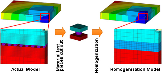
Introduces an analysis example applied to the actual model by evaluating the equivalent property value based on the result of numerical material test by cutting the cycle symmetry structure of the solder.
Analysis Results
Macro structural analysis of the electronic substrate
Printed circuit board is a representative example of the object to be analyzed and it is difficult to conduct structural analysis with high accuracy because of the complexity of the fine structure. However, it is possible to simplify microstructure with small scale by using CMAS, if it has non-uniform geometric characteristics arrayed periodically such as solder. Images are as shown below, and the distribution of the stress/strain of the micro-scale considering the non-uniformity will result in the average by homogenizing the heterogeneous structure.
Numerical material test of non-homogeneous microstructure model
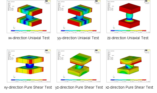
Performing the material test virtually (numerical material test) to cyclic symmetry structure using ANSYS in CMAS in order to homogenize the solder area mentioned above. In the virtual test, you do not need to create a test piece shape conforming to the JIS standard. It can give a stress field in the ideal model of the unit cell by defining internally particular boundary conditions. An equivalent material property value to simplify the non-uniformity will be calculated by the results of this material test and will evaluate the response of strain and apparent stress. In this analysis case, it has been applied to the actual structure model by homogenizing the linear expansion coefficient and orthotropic elastic modulus.
Analysis Types
Structural Analysis、Multiscale Analysis、Macro Structural Analysis