


OLED Methodology
INTRODUCTION
|
Light emitting diodes (LED) and organic light emitting diodes (OLED) employ intricate materials and nano structures for enhanced performance. Modeling these devices requires accounting for incoherent response and optimizing numerous design parameters simultaneously. This often entails extensive simulations. Our approach involves using 1D analytical methods to capture interference and microcavity effects swiftly. In 2D, we utilize FDTD to sweep design parameters and dipole positions, extracting key metrics like light extraction efficiency. Symmetry methods are employed to expedite 3D FDTD simulations for final parameter verification. An overview of relevant metrics and exporting results to raytracing software is provided. |
|
1D Multilayer Stacks
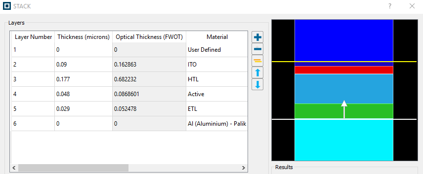
Analytical methods excel in swiftly calculating optical responses for unpatterned planar OLEDs/LEDs, outpacing direct Maxwell's equations simulations. Lumerical's STACK Solver offers efficient 1D optical STACK functions, swiftly capturing interference and microcavity effects, providing results within seconds for rapid device analysis.
Layer thickness and dipole position
Access the STACK solver via script commands or the GUI based on user preference. Define stack properties using GUI options or n (index) and d (thickness) vectors. Indices can be C numbers or material names from the library.
Enhance spontaneous emission by maximizing field intensity in the active region, using Stackfield to assess multiple wavelengths simultaneously. Alternatively, suppress emission for color adjustment. For far-field power density analysis, utilize Stackpurcell, sweeping dipole position through the active layer. LEDs, with complex dimensions, benefit from STACK for far-field power distribution analysis.
Slab mode analysis
|
Gain insight into substrate radiation propagation via FDE mode structure analysis. Relevant for mode support and outcoupling. FDE models lossy, dispersive materials for bandwidth sweep. |
|
2D Patterned Structure
FDTD, a potent optical solver, adeptly models wavelength-scale patterning's impact on device efficiency, crucial for OLED and LED simulations. Designs with thin layers of dispersive materials often employ intricate patterning to enhance quantum efficiency.
Structure
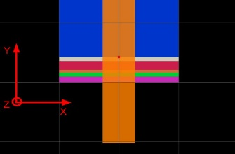
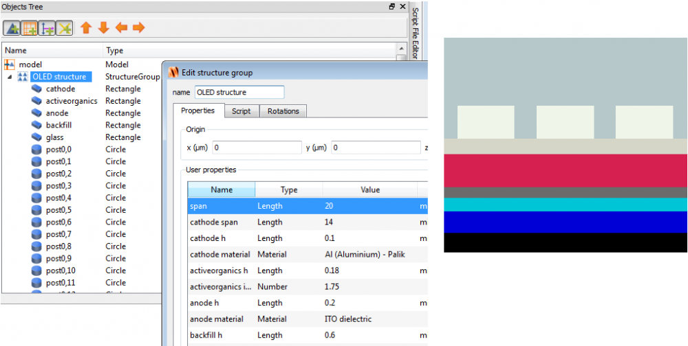
The conventional OLED layers can be constructed using rectangles. OLED patterning should be parameterized using a structure group, which allows one to sweep the design parameters to achieve optimal efficiency.
Simulation region
Use PML boundaries on all sides except under the metallic cathode layer, where a metal boundary condition may be suitable. Ensure the simulation span is large enough to cover multiple patterning periods tangentially and avoids near-field interactions with PML boundaries normal to the plane of substrate. Avoid periodic boundary conditions due to the structure's periodicity. Start with low mesh accuracy for easier debugging. Enhance simulation efficiency with coarse mesh override regions.
Sources: simulating incoherent, isotropic emission
OLED/LED active regions optimize spontaneous emission through electron-hole recombination or molecular transitions. Generated photons exhibit random direction, phase, and polarization, hence incoherent. Despite requiring quantum mechanics for precise treatment, electromagnetic point dipole sources allow classical analysis. FDTD requires three separate simulations for dipole orientations, and dipole positions must sweep through the active layer, resembling statistical sampling to converge on the true incoherent response. Increasing sample size reduces confidence interval.
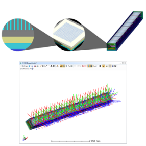
3D Final Parameter Extraction
While 2D OLED models provide insights, final verification with experiments often requires 3D simulations. Though like 2D, 3D simulations are memory and time-intensive. We present methods to enhance throughput, crucial for OLEDs due to the need to sweep source position and orientation.
Structure and simulation region.
When conducting 2D simulations, it's essential to parameterize the structure and develop material models that accurately represent the optical properties of the layers. Properly implement PML for boundaries.
Sources and symmetry
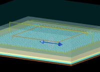
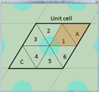
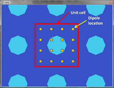
To model the device's incoherent nature, multiple dipole positions and orientations are swept. A predefined grid or random selection is used. For example, a 4x4 grid entails 48 simulations, with 3 orientations per dipole. Automation via parameter sweep tool or scripting is recommended. Symmetry in the device can significantly decrease simulation numbers, a process outlined further ahead.
|
Hexagonal lattice symmetry |
Square lattice symmetry |
Interface with Ray Tracing
See the following example for more information on exporting ray sets to geometric optical solvers.
|
|
|

Original content credit: Ansys Canada Ltd.
Contact us for more details about optical simulation using Ansys software